
Logic Gates
Welcome to this Verilog Fundamentals tutorial series. In the previous article, we introduced EDA Playground [2] and walked through the complete simulation workflow: writing a Verilog module, writing a testbench, running Icarus Verilog, reading the console output, and viewing signal traces in EPwave. With that workflow established, this article introduces the five fundamental logic gates, NOT, AND, OR, NAND, and NOR, with their schematic symbols and truth tables. De Morgan’s law is then explained, showing why NAND and NOR are universal gates. The article concludes with two gate-level Verilog examples run in EDA Playground: a demonstration that two NAND gates in series produce AND behaviour, and a 2-to-1 multiplexer assembled from NOT, AND, and OR gate primitives.
Logic Gates
Logic gates are the building blocks of all digital electronics. Think of each gate as a tiny decision-maker: it looks at one or more input signals and produces one output signal based on a fixed rule. Every input and output has only two possible states, which engineers call HIGH and LOW. HIGH means the voltage is near the top of the circuit’s supply, and LOW means it is near zero volts. In everyday terms, HIGH is on and LOW is off, just like a light switch. The supply voltage on an FPGA is typically 1.8 V, 3.3 V, or 5 V depending on the device and the logic bank, but the high-or-low distinction is all that matters for understanding what each gate does. In this article, gate names are capitalised for emphasis, and this is also the convention in digital electronics literature.
The NOT Gate
The simplest logic gate is the NOT gate. It is also called an inverter. It has one input and one output, and its rule is the simplest of all: it always does the opposite of what comes in. If the input is high, the output is low. If the input is low, the output is high. Think of it like a light switch with a twist: pressing it turns the light off if it was on, or on if it was off.
The schematic symbol for the NOT gate is shown in the illustration below. Notice the small circle at the output tip of the symbol. That little circle is the universal sign for inversion in electronics schematics and will appear again on other gates later in this article. Below the symbol is the truth table for the NOT gate. A truth table is a complete list of every possible input combination and the output that results. Because the NOT gate has only one input, the truth table has just two rows, one for each possible input state. By convention, inputs are labelled starting at the beginning of the alphabet using names such as A, B, and C. Outputs are often labelled Q or letters near the end of the alphabet such as X, Y, and Z.
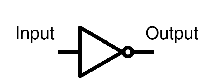
| A | Q |
|---|---|
| 0 | 1 |
| 1 | 0 |
In Verilog, the NOT gate is available as a built-in primitive. The output port comes first in the port list, followed by the input:
// Verilog -- NOT gate primitive
not G1 (q, a);   // q = NOT a
The instance name G1 is optional but helps trace signals during simulation. Any number of NOT primitives can be instantiated in the same module with different instance names.
The AND Gate
The AND gate has two or more inputs and one output. Its rule is that the output is high only when every single one of its inputs is high at the same time. If any input is low, the output goes low too. Think of it like a bicycle lock with two separate key slots: both keys must be inserted and turned before the lock opens. One key on its own is not enough.
The schematic symbol for a two-input AND gate is shown in the illustration below, followed by its truth table. The truth table has four rows because with two inputs there are four possible combinations. Notice that the output is 1 only in the last row, where both A and B are 1.
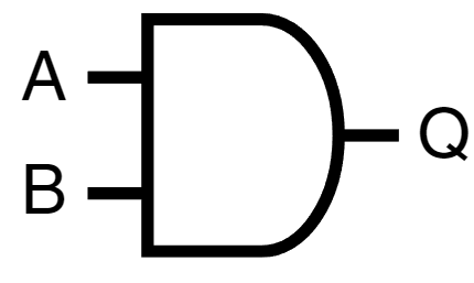
| A | B | Y |
|---|---|---|
| 0 | 0 | 0 |
| 0 | 1 | 0 |
| 1 | 0 | 0 |
| 1 | 1 | 1 |
In Verilog, the AND gate primitive places the output first, followed by all inputs:
// Verilog -- AND gate primitive
and G1 (y, a, b);   // y = a AND b
Adding a third port, and G1 (y, a, b, c), gives a three-input AND gate with no extra wiring. Synthesis tools map any number of inputs directly to the target hardware.
The OR Gate
The OR gate also has two or more inputs and one output. Its rule is the opposite of the AND gate: the output is high if any of its inputs is high. It does not matter which input is high or how many are high, so long as at least one is. Think of it like a car alarm that can be triggered by the door sensor, the bonnet sensor, or the motion sensor: any one of them firing is enough to set it off.
The schematic symbol for a two-input OR gate is shown in the illustration below, and its truth table follows. Notice that the output is 0 only in the first row, where both A and B are 0. Every other combination gives an output of 1.
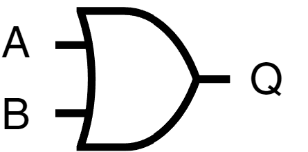
| A | B | Y |
|---|---|---|
| 0 | 0 | 0 |
| 0 | 1 | 1 |
| 1 | 0 | 1 |
| 1 | 1 | 1 |
In Verilog, the OR gate primitive follows the same output-first port convention:
// Verilog -- OR gate primitive
or G1 (y, a, b);   // y = a OR b
Like the AND primitive, additional inputs can be added as extra ports. The output goes high as soon as any one of the inputs is high.
NAND and NOR Gates
NAND stands for NOT AND, and NOR stands for NOT OR. These gates work exactly as their names suggest: a NAND gate is an AND gate with its output flipped, and a NOR gate is an OR gate with its output flipped. Recall the small circle on the output of the NOT gate symbol seen earlier. That same circle appears on the NAND and NOR symbols to show that the output has been inverted. Compare the NAND symbol and truth table with the AND gate above: every output entry is the opposite.
The schematic symbols and truth tables for both gates are shown in the illustrations below.
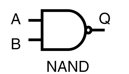
| A | B | Y |
|---|---|---|
| 0 | 0 | 1 |
| 0 | 1 | 1 |
| 1 | 0 | 1 |
| 1 | 1 | 0 |
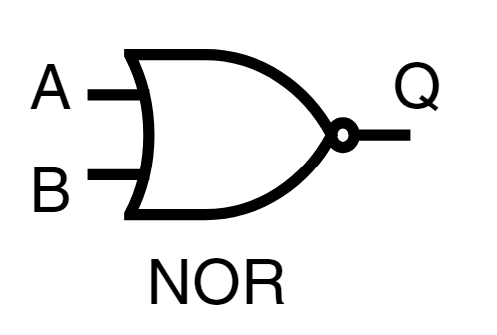 |
| A | B | Y |
|---|---|---|
| 0 | 0 | 1 |
| 0 | 1 | 0 |
| 1 | 0 | 0 |
| 1 | 1 | 0 |
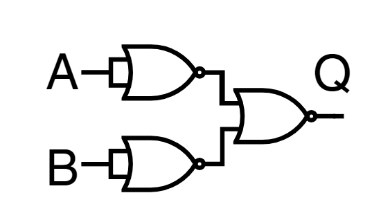
Both NAND and NOR gates are described as universal gates because either one of them alone is enough to build any other type of logic gate. To make a NOT gate from a NAND or NOR gate, simply connect both inputs to the same signal. The diagram below shows how three NOR gates can be wired together to produce the behaviour of a single AND gate.
Both primitives follow the same output-first port order used by AND and OR:
// Verilog -- NAND and NOR gate primitives
nand G1 (y, a, b);   // y = NOT(a AND b)
nor  G2 (y, a, b);   // y = NOT(a OR b)
Tying both inputs of a NAND gate to the same signal produces a NOT function: nand G1 (q, a, a) gives q = NOT a. This is the tied-input trick that makes NAND and NOR universal, and Example 1 demonstrates the NAND version in simulation.
De Morgan’s Law
The three-NOR-gate construction in the diagram above makes use of a rule called De Morgan’s law. This law is easier to grasp by starting with plain English. Consider the statement “it is NOT the case that A is true AND B is true.” De Morgan’s law tells us that this is exactly the same as saying “either A is NOT true, OR B is NOT true.” In other words, flipping the result of an AND is the same as flipping each individual input and using OR instead. That is exactly what the NOR-gate AND construction does: each input is individually inverted by a NOR gate with its inputs tied together, those inverted signals are OR-combined, and then the combined result is inverted again, giving the overall effect of AND-ing the original inputs. Once this pattern is clear, it is not hard to see why NAND and NOR are called universal gates. Any logic function, no matter how complex, can be broken down and rebuilt using only one of them.
De Morgan’s law has two equivalent forms. The first states that NOT(A AND B) equals (NOT A) OR (NOT B). The second states that NOT(A OR B) equals (NOT A) AND (NOT B). Together these two forms mean that any logic function built from AND, OR, and NOT can be rebuilt entirely from NAND gates alone, or entirely from NOR gates alone, because a NAND gate is NOT layered on top of AND, and a NOR gate is NOT layered on top of OR.
Substituting values confirms the first form. With A equal to 1 and B equal to 0, the left side gives NOT(1 AND 0) = NOT(0) = 1, and the right side gives (NOT 1) OR (NOT 0) = 0 OR 1 = 1. Both produce the same result. With A and B both equal to 1, the left side gives NOT(1 AND 1) = NOT(1) = 0, and the right side gives (NOT 1) OR (NOT 1) = 0 OR 0 = 0. Again both sides agree. The equality holds for all four combinations of A and B, which is the full content of the first form. The second form can be verified the same way: substituting each row of the OR truth table into NOT(A OR B) and (NOT A) AND (NOT B) produces identical results in every case.
The NAND-gate form of a plain AND function follows directly from the first form of the law. A single NAND gate computes NOT(A AND B). Tying both inputs of a second NAND gate to the first gate’s output inverts that result, producing NOT(NOT(A AND B)), which simplifies to A AND B. Gate-level Verilog makes this construction explicit in code, and the first example below implements it so that the equivalence can be confirmed in simulation.
Gate-level modelling
Gate-level modelling is the style of Verilog in which a design is described by instantiating named logic-gate primitives and connecting them with wires, directly mirroring a circuit schematic. Verilog provides built-in primitives for all five gates covered in this article: not, and, or, nand, and nor. Each primitive is instantiated with an optional instance name followed by the port connections in output-first order. The two examples below build complete gate-level modules and verify them in EDA Playground using the workflow established in the previous article.
Example 1: Constructing an AND Gate from NAND Gates
This example implements the De Morgan’s law construction described above: two NAND gates connected in series to produce AND behaviour. The diagram below shows the equivalent construction using NOR gates; the NAND version follows exactly the same principle applied to the other universal gate.
The first gate, G1, accepts inputs a and b and drives an internal wire nand_out with NOT(A AND B). The second gate, G2, takes nand_out on both its input connections, which is equivalent to a NOT gate, and drives the output y with the final AND result.
Enter the following module in the Design panel in EDA Playground:
// Verilog -- AND gate constructed from two NAND gates
module nand_and(
    input  a, b,
    output y
);
    wire nand_out;
    nand G1 (nand_out, a, b);          // first NAND: NOT(A AND B)
    nand G2 (y, nand_out, nand_out);   // second NAND as NOT: inverts G1 output
endmodule
The port list for each primitive places the output first, followed by the inputs. Gate G1 therefore writes to nand_out and reads from a and b. Gate G2 writes to y and reads nand_out on both input positions, effectively inverting it. Tracing the logic for the case where both a and b are 1 confirms the construction: G1 produces 0, and G2 inverts 0 to produce 1 on y, matching the AND truth table row for A=1, B=1.
Testbench
Enter the following testbench in the Testbench panel:
// Verilog -- testbench for nand_and module
module nand_and_tb;

    reg  a, b;
    wire y;

    nand_and uut (
        .a(a),
        .b(b),
        .y(y)
    );

    initial begin
        $dumpfile("nand_and.vcd");
        $dumpvars(0, nand_and_tb);
    end

    initial begin
        $display("Time\t a\t b\t y");
        $monitor("%0t\t %b\t %b\t %b", $time, a, b, y);

        a = 0; b = 0; #10;
        a = 0; b = 1; #10;
        a = 1; b = 0; #10;
        a = 1; b = 1; #10;

        $finish;
    end

endmodule
The testbench applies all four input combinations in order, stepping through the complete AND truth table. The $monitor task prints a line each time any signal changes value, so the console log reflects the output y for every combination as it is applied. The nand_and module is instantiated as uut (unit under test), following the same convention used in the previous article.
Running the Simulation
Select Icarus Verilog as the simulation tool, tick the “Open EPWave after run” checkbox, and click Run. The console output for a correctly entered design and testbench will be:
Time     a       b       y
0        0       0       0
10       0       1       0
20       1       0       0
30       1       1       1
The output y is high only at time 30, when both a and b are 1. This matches the AND truth table and confirms that two NAND gates reproduce AND behaviour. In EPwave, after adding a, b, and y to the waveform display and clicking Zoom to Fit, the y trace will appear as a flat low line for the first three time intervals and rise to high only during the final interval, providing a visual confirmation of the gate construction.
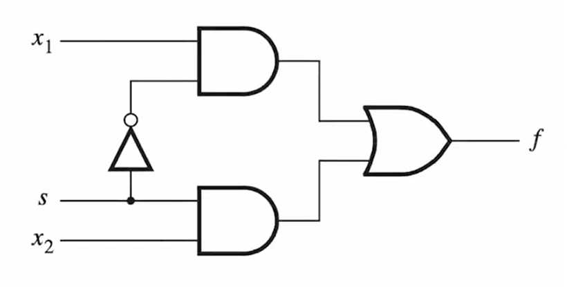
Example 2: A 2-to-1 Multiplexer
A multiplexer selects one of several data inputs and routes it to a single output. A 2-to-1 multiplexer has two data inputs x1 and x2, a selector input s, and one output f. When s is 0, the output follows x1; when s is 1, the output follows x2. The gate-level circuit that produces this behaviour uses a NOT gate, two AND gates, and one OR gate, as shown in the circuit diagram below.
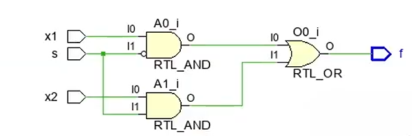
Enter the following module in the Design panel:
// Verilog -- 2-to-1 multiplexer using gate primitives
module mux_2x1_gate(
 input x1, x2, s,
 output f
);
 not (sn, s);
 and A0 (g0,x1,sn);
 and A1 (g1,x2,s);
 or O0 (f, g0, g1);
endmodule
The NOT gate produces sn, the complement of the selector s. Gate A0 drives g0 with x1 when sn is high, which is when s is 0. Gate A1 drives g1 with x2 when s is high. Because s and sn are always opposite values, at most one AND gate is active at any time, so only one data input reaches the OR gate and appears on f. The figure below shows the assembled circuit as it would appear on a schematic.
The multiplexer is a more instructive example than the NAND-to-AND construction because it cannot be reduced to a single primitive gate. It requires four gate instances working together: the NOT gate inverts the selector, the two AND gates gate each data input, and the OR gate combines both results into the output. This pattern of smaller gates composed into a larger function is the foundation of all gate-level digital design. Every combinational circuit on an FPGA, however complex, is ultimately a network of primitives connected by wires, and the gate-level Verilog style in this example is a direct, one-to-one representation of that network. Understanding this composition at the gate level makes it straightforward to read and verify the higher-level design styles introduced in the next episode.
Testbench
Enter the following testbench in the Testbench panel:
// Verilog -- testbench for mux_2x1_gate module
module mux_2x1_gate_tb;

    reg  x1, x2, s;
    wire f;

    mux_2x1_gate uut (
        .x1(x1),
        .x2(x2),
        .s(s),
        .f(f)
    );

    initial begin
        $dumpfile("mux_2x1_gate.vcd");
        $dumpvars(0, mux_2x1_gate_tb);
    end

    initial begin
        $display("Time\t x1\t x2\t s\t f");
        $monitor("%0t\t %b\t %b\t %b\t %b", $time, x1, x2, s, f);

        x1 = 0; x2 = 0; s = 0; #10;
        x1 = 1; x2 = 0; s = 0; #10;
        x1 = 0; x2 = 1; s = 1; #10;
        x1 = 0; x2 = 0; s = 1; #10;

        $finish;
    end

endmodule
The four test vectors exercise the selector in both states with different data input values. The first two vectors hold s at 0 to verify that f tracks x1. The last two vectors set s to 1 to verify that f tracks x2.
Running the Simulation
With Icarus Verilog selected and EPWave enabled, click Run. The expected console output is:
Time     x1      x2      s       f
0        0       0       0       0
10       1       0       0       1
20       0       1       1       1
30       0       0       1       0
At time 0, all inputs are 0 and f is 0. At time 10, x1 rises to 1 while s remains 0, so f follows x1 to 1. At time 20, s switches to 1 and x2 rises to 1, so f follows x2 and remains at 1. At time 30, x2 returns to 0 while s stays at 1, and f drops to 0 tracking x2. In EPwave, the f trace will mirror the x1 trace during the first two time intervals and switch to mirroring the x2 trace when s goes high, showing the selector handoff as a clear transition point on the waveform.
What Comes Next
This article has moved from reading gate symbols and truth tables to writing and simulating gate-level Verilog. The NAND-to-AND example grounded De Morgan’s law in runnable code. The multiplexer example showed how four gate primitives combine to route one of two data inputs to an output based on a selector signal. Both designs are purely combinational: the output at any moment depends only on the current inputs, with no memory of previous states.
The next episode covers three additional Verilog design styles, each describing the same combinational logic at a different level of abstraction. Dataflow modelling uses continuous assign statements and logical operators, expressing what value each signal should hold rather than which gates connect. Behavioural modelling uses procedural always blocks with conditional statements, bringing the code closer to a conventional programming language while remaining synthesisable to hardware. Hierarchical design connects modules inside other modules, so that a larger circuit can be assembled from verified sub-components exactly as one would build a system from individual parts. Each style has its strengths, and knowing when to reach for each one is a core skill in Verilog design.
References
[1] Maxfield, C. Programming FPGAs: Getting Started with Verilog. McGraw-Hill, 2017. Cited for gate schematic symbols, truth tables, universal gate constructions, the De Morgan’s law example circuit, and the 2-to-1 multiplexer gate-level design used in this article.
[2] “EDA Playground.” Doulos, 2012–present. Available at https://www.edaplayground.com/. Cited for the browser-based Verilog simulation environment used to run both gate-level examples in this article.
Glossary
AND gate: A logic gate whose output is high only when all of its inputs are simultaneously high; in this article demonstrated with a schematic symbol, a truth table, and a two-NAND-gate Verilog construction in Example 1.
combinational logic: Digital logic whose output at any moment depends only on its current inputs, with no memory of previous states; both Verilog examples in this article describe combinational circuits.
De Morgan’s Law: A pair of logical equivalences stating that NOT(A AND B) equals (NOT A) OR (NOT B), and that NOT(A OR B) equals (NOT A) AND (NOT B); used in this article to explain the universal-gate property of NAND and NOR gates and to derive the NAND-to-AND construction in Example 1.
EDA (Electronic Design Automation): A category of software tools for designing and simulating electronic circuits; in this series, refers to EDA Playground, the browser-based Verilog simulator used to run both gate-level examples.
FPGA (Field-Programmable Gate Array): An integrated circuit whose internal logic can be configured after manufacture by loading a hardware description; the target device for Verilog designs throughout this series, and the source of the supply voltage values discussed in the Logic Gates section.
gate-level modelling: A style of Verilog design in which a circuit is described by instantiating named gate primitives and connecting them with named wires, mirroring a circuit schematic; used for both Verilog examples in this article.
HDL (Hardware Description Language): A programming language used to describe the structure and behaviour of digital electronic circuits; Verilog is the HDL used throughout this series.
mux (2-to-1 multiplexer): A combinational circuit that routes one of two data inputs to a single output based on the state of a selector input; in this article, implemented as a gate-level Verilog module using not, and, and or primitives and verified in EDA Playground.
NAND (NOT AND): A logic gate whose output is low only when all of its inputs are simultaneously high, equivalent to an AND gate followed by a NOT gate; described in this article as a universal gate and used in Example 1 to construct an AND gate.
NOR (NOT OR): A logic gate whose output is high only when all of its inputs are simultaneously low, equivalent to an OR gate followed by a NOT gate; described in this article as a universal gate alongside NAND.
NOT gate: A logic gate with one input and one output whose output is always the logical inverse of its input; also called an inverter, and used in Verilog via the not primitive.
OR gate: A logic gate whose output is high when one or more of its inputs are high; used in the 2-to-1 multiplexer to combine the outputs of the two AND gates into the final output signal f.
testbench: A Verilog module written to drive a design under test with input signals and observe the resulting outputs; both examples in this article use testbenches that apply all relevant input combinations and print results to the console via $monitor.
truth table: A table listing every possible combination of binary input values for a logic gate or circuit and the corresponding output for each combination; used in this article to define the expected behaviour of all five gate types.
universal gate: A logic gate from which every other logic gate can be constructed using only that gate type; both NAND and NOR are universal gates, as explained in the De Morgan’s Law section and demonstrated in Example 1.
VCD (Value Change Dump): A standard file format that records how digital signals change over simulated time; produced by Icarus Verilog via the $dumpfile and $dumpvars system tasks in the testbench, and read by EPwave to draw the signal waveform traces.