Using EDA Playground
Welcome to this Verilog Fundamentals tutorial series. Verilog is the programming language that transforms hardware description into a programming language. It is literally called a Hardware Description Language (HDL). But wait a minute, “what exactly do you mean by hardware?” one might ask. Well, that is a very good question, because hardware could mean almost anything, right? Yes, well, generally speaking, if we break the word hardware into two (the linguistic exercise known as morphology), we get “hard” and “ware”. So we can loosely translate hardware as being “hard” “things” or “hard (solid) stuff”. Notwithstanding, within the Engineering domain, “hardware” has the more specific meaning of electronics, or at least the part of electronics that is not software. So in general, electronics engineering is split into the two sub-fields of electronics hardware engineering and electronics software engineering. We already know what software means, right? These are the programs we run on our computers. In order to work, however, software needs some hardware to run on, which does not particularly help our intuition of the subject of hardware versus software. That said, hardware description languages like Verilog do not describe all electronics hardware. Only a subset of electronic hardware is described by HDLs. This subset is called digital electronics. So Verilog is a HDL that describes digital electronics in a software programming language fashion. Although this further blurs the lines of distinction between hardware and software, and as confusing as this may sound, there are justifiable reasons to do this. The main advantage of describing hardware in software is the economy involved in producing pure hardware versus soft hardware. In other words, it is a lot cheaper, faster, more efficient, and ultimately more economical to produce hardware as software versus pure hardware. We avoid going down the rabbit hole any further so as not to spawn a different article entirely.
Anyway, with the little introductory note on why Verilog out of the way, and if Verilog is something of interest, then let us dive into what is in store for us today in this article.
Prerequisites and Equipment
The focus for today is the tools and resources required to get started programming in Verilog. Before diving into the tools, one first needs to consider what prerequisite knowledge is required to program in Verilog. Usually, HDL is a subject taught at undergraduate level electronics, and it probably carries a higher learning curve than that of hobbyist electronics. That said, this article series attempts to make the material accessible to anyone with a high (secondary) school education.
The first piece of equipment one would require to program in Verilog is a computing device. If one is reading this online, there is probably already access to a computing device, whether that is a desktop, laptop, or mobile phone. In this series of articles, all of the above devices are supported. That said, the best experience will be found using either a desktop computer or a laptop computer. There is no guarantee that all the necessary tools will run on all of these devices, and the mobile phone will have the most limited support of the three.
Software CAD Tools
The remainder of this tutorial focuses on the software tools one will require to write and run Verilog programs. There are two paths to choose from. The first path is the one to follow for those who prefer to develop using an actual FPGA training board. Going down this route enables programming the training board with Verilog and allows experimentation with the results of a program usable on the FPGA board of choice. This will be of interest to those who love to experiment with hands-on exercises using physical devices. This is, however, the more expensive route, requiring the purchase of an FPGA development board. The other choice is using an HDL simulator. For this route, the EDA Playground online HDL simulator is the tool of choice. This series of tutorials has been designed to support both paths by providing parallel versions of the tutorials. If one prefers using an FPGA board, note that the software requirements are board specific. This series of tutorials uses Xilinx boards and Vivado software. However, there are other non-Xilinx boards using alternative software CAD tools. The most common would be Intel FPGA Altera devices and the accompanying Intel Quartus software. These other FPGA devices and their accompanying software follow similar Verilog development workflows, so it is entirely possible to follow along using those alternative platforms. However, only the details of Vivado and Xilinx will be covered in this series, and in particular this series of tutorials uses the Xilinx Basys3 development board. Newcomers may find these constraints somewhat challenging, and hence using the FPGA simulation path is the recommended starting point.
Conversely, if one decides to follow the FPGA simulation path, this is the path likely to have the widest coverage of readers of this blog series in terms of cost and platform compatibility. Also note that there are several simulation tools that can achieve the same goals as EDA Playground. For instance, Intel FPGA software ships with the ModelSim program, which performs FPGA simulation. However, here the focus will be on EDA Playground, as the online capability of using mobile browsers gives the mobile user some level of experimentation, even though it is not the ideal experience. Moreover, the online browser experience simplifies the setup process without the need to install any software at all. Having a web browser on the computing device is sufficient to get started programming Verilog.
Note: FPGA Simulation Track
From this point forward, this article covers the FPGA simulation track exclusively. All instructions assume that one has access to a web browser and a working internet connection. No additional hardware or software installation is required. If one already has access to a Xilinx Basys3 or similar Xilinx development board, or prefers to follow the physical hardware path, the FPGA board track is covered in the parallel Episode 1 article in this series, which walks through the same Verilog concepts using the Vivado design suite and a real FPGA device. One can return to this article and the simulation track at any point once a preference for one path or the other has been established.
Getting Started with EDA Playground
EDA Playground is a free, browser-based environment for writing and simulating HDL designs. It requires no installation and no local software of any kind. All that is needed is a web browser and, for saving work between sessions, a free account. The simulation backend used throughout this series is Icarus Verilog, which is a widely used open-source Verilog compiler and simulator that handles standard Verilog reliably across a broad range of designs. EDA Playground also integrates the EPwave waveform viewer, which displays simulation results as signal traces and provides a visual representation of how signals change over simulated time. Together, Icarus Verilog and EPwave cover everything needed to write, run, and inspect a Verilog simulation without leaving the browser.
Creating an Account
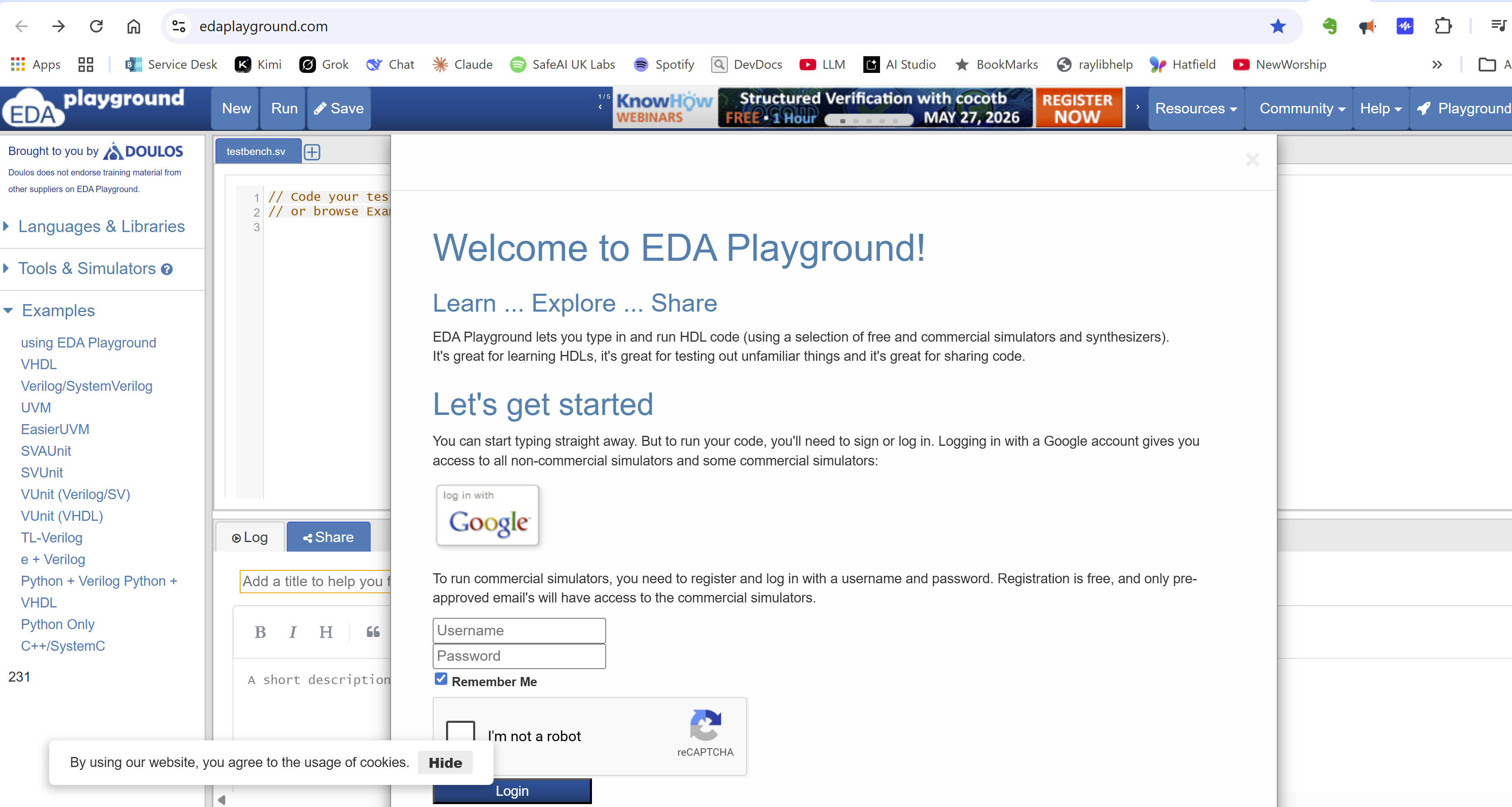
Navigate to EDA Playground in a web browser. On the home page, locate the “Sign In” link at the top right of the page and click it. One can create a free account using either a Google account or an email address. If using Google, click “Sign in with Google” and follow the authorisation prompts. If using an email address, click “Register” and complete the registration form with a name, email address, and password. Account creation is free and takes less than a minute.
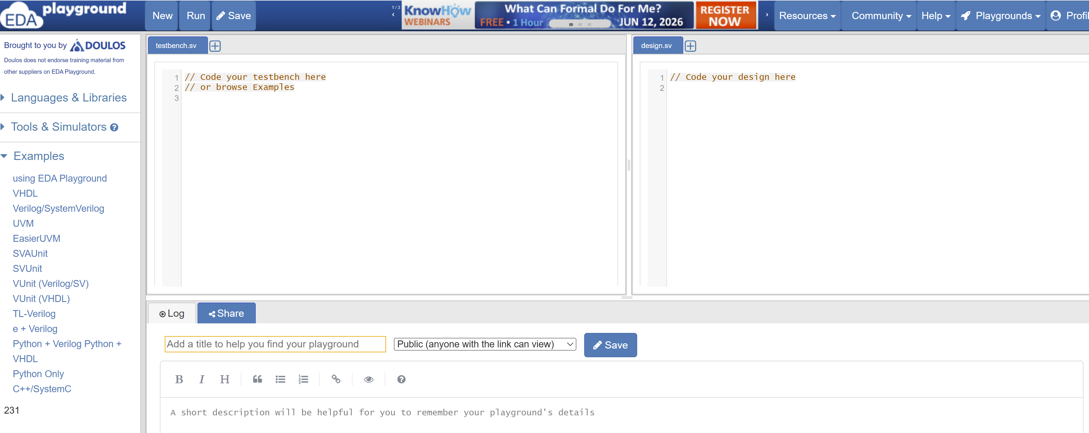
Once signed in, the EDA Playground editor opens. The interface consists of two large text panels side by side. The left panel is labelled “Design” and accepts the Verilog design file. The right panel is labelled “Testbench” and accepts the simulation testbench. Below these panels are the simulator configuration options, the Run button, and the log output area. All the tools needed to write, configure, and run a simulation are visible in a single browser window.
Creating a New Playground
In the top toolbar, locate the “New” button to open a fresh playground. Give it a descriptive name so that it is easy to retrieve later; for this first project, “switch_led” is a suitable name. EDA Playground saves work automatically to the account when one is signed in, so there is no need to save manually between edits. Each playground holds one design file and one testbench file, which maps directly to the two-panel structure of the editor and to the two-file structure used throughout this tutorial series.
Configuring the Simulator
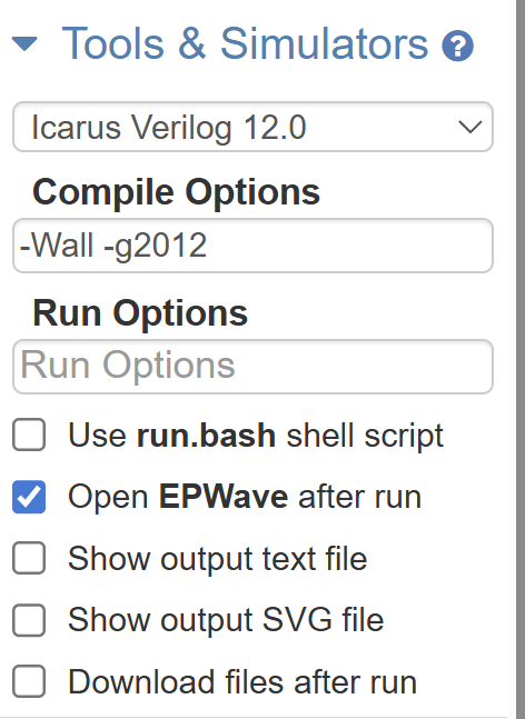
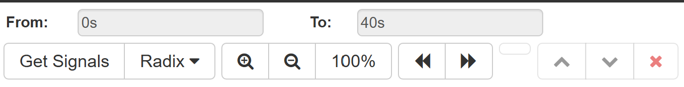
Below the two editing panels, locate the simulator configuration row. From the left-side dropdown, under the Tools & Simulation section select “Icarus Verilog” as the simulation tool. On the right side of the same row, ensure that the “Open EPWave after run” checkbox is ticked. This setting causes the EPwave waveform viewer to open automatically in a new browser tab after each simulation run, displaying the signal traces generated by the design. Without this checkbox ticked, the waveform file is still generated during the simulation, but it must be opened manually from the log area. Ticking it once is sufficient; EDA Playground remembers the setting for the current playground session.
Your First Simulation: Switch to LED
With EDA Playground configured, one is ready to build and simulate the first Verilog design. This project simulates the same switch-to-LED connection described in the parallel Episode 1 article. A slide switch drives an LED: when the switch is set to 1, the LED turns on; when it is set to 0, the LED turns off. It is the simulation equivalent of the hardware board project, and it demonstrates the complete simulation workflow from writing a Verilog module to viewing the results as a waveform.
Entering the Verilog Module
In the Design panel on the left, delete any placeholder content and enter the following Verilog module:
// Verilog -- connect slide switch SW0 to LED LD0 on the Basys3 board
module switch_led(
    input  wire sw,    // connected to slide switch SW0
    output wire led    // connected to LED LD0
);
    assign led = sw;

endmodule
This is exactly the same module used in the FPGA board track. It contains no board-specific content: there are no pin assignments, no electrical standard declarations, and no reference to any particular FPGA device. The module declares two ports and connects them with a continuous assign statement, meaning the output led will always reflect the current state of the input sw. Because the module is pure RTL (register-transfer level) Verilog, it runs equally well in a simulator or on real hardware. The XDC constraints file used in the board track is not needed here; the simulator does not interact with physical pins and requires no information about which pin is wired to which signal on the board.
Writing the Testbench
A testbench is a Verilog file that exercises a design under test by applying inputs and observing outputs. In the physical board track, one flips a slide switch and watches an LED respond; in simulation, the testbench takes on both roles, acting as the switch and as the observer. Enter the following testbench in the Testbench panel on the right:
// Verilog -- testbench for switch_led module
module switch_led_tb;

    reg  sw;   // driven by the testbench, so declared as reg
    wire led;  // driven by the module under test, so declared as wire

    // Instantiate the design under test
    switch_led uut (
        .sw(sw),
        .led(led)
    );

    // Set up waveform dumping for EPwave
    initial begin
        $dumpfile("switch_led.vcd");
        $dumpvars(0, switch_led_tb);
    end

    // Apply test vectors and print results to the console
    initial begin
        $display("Time\t sw\t led");
        $monitor("%0t\t %b\t %b", $time, sw, led);

        sw = 0; #10;  // switch off, wait 10 time units
        sw = 1; #10;  // switch on,  wait 10 time units
        sw = 0; #10;  // switch off, wait 10 time units
        sw = 1; #10;  // switch on,  wait 10 time units

        $finish;      // end the simulation
    end

endmodule
Several points in this testbench are worth noting. The input to the module, sw, is declared as reg because the testbench drives it directly. The reg type holds a value between assignments, which models a switch that stays in a fixed position until explicitly moved. The output led is declared as wire because the module under test drives it, not the testbench. The line switch_led uut (...) instantiates the design under test, and the conventional name uut stands for “unit under test”. The $dumpfile and $dumpvars system tasks instruct Icarus Verilog to record all signal activity to a file named switch_led.vcd; this VCD (Value Change Dump) file is what EPwave reads to draw the waveform. The $display system task prints a single header line at the start of the simulation. The $monitor system task prints a new line each time any of the listed signals changes value, so the console log will show the exact simulation time and signal state at every transition. The #10 delay operator advances simulation time by ten time units, giving each switch state enough simulated duration to appear as a distinct region on the waveform.
Running the Simulation
With both panels populated, click the “Run” button located below the editing panels. EDA Playground submits the design and testbench to the Icarus Verilog compiler. After a few seconds, the log area at the bottom of the page will populate with compiler and simulation output. If there are any syntax errors in the Verilog, the compiler will report them here with line numbers identifying each problem. For a correctly entered design and testbench, the log area will show the simulation console output, confirm that the VCD file has been written, and note that EPwave has been launched in a new browser tab.
Reading the Console Output
The $monitor statement in the testbench produces a line of console output each time sw or led changes value. For the test sequence written above, the expected output in the log area is:
Time     sw      led
0        0       0
10       1       1
20       0       0
30       1       1
The first data line corresponds to the state at time zero, where sw is assigned 0 and led follows immediately. At time 10, sw is set to 1, and led responds in the same simulation step, confirming that the continuous assign connection is working. The pattern repeats at times 20 and 30. The fact that sw and led change at exactly the same time step is expected for a purely combinational connection with no propagation delay modelled. Checking this table against the test vectors written in the testbench is a useful first verification before turning attention to the waveform.
Viewing the Waveform in EPwave
After the simulation completes, EPwave opens automatically in a new browser tab if the “Open EPWave after run” checkbox was ticked. The EPwave interface has a scope panel on the left and a waveform display area to the right. The scope panel lists all the signals recorded in the VCD file.
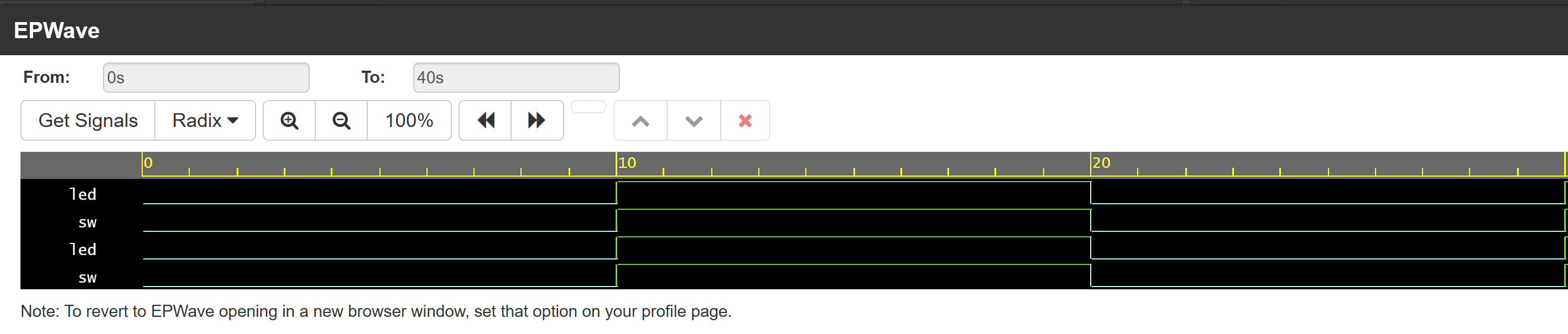
To add signals to the waveform display, locate sw and led in the scope panel and drag them into the waveform area. Alternatively, right-click each signal name and select “Add to Wave”. Once both signals appear as rows in the waveform area, click “Zoom to Fit” in the toolbar at the top to scale the display so that the entire simulation time range is visible at once.
The waveform display will show two horizontal signal rows. The sw trace alternates between low (0) and high (1) at regular ten-unit intervals, following the test sequence written in the testbench. Directly below it, the led trace follows sw exactly, with no visible gap between the two transitions. This visual confirmation that the output tracks the input is the waveform equivalent of flipping slide switch SW0 on the Basys3 board and watching LED LD0 respond. For more complex designs the waveform view becomes indispensable: it makes it straightforward to spot unexpected behaviour such as glitches, delayed transitions, or signals that fail to change at all. Developing the habit of inspecting waveforms alongside console output from the very first project means one is well prepared for the more intricate designs that follow in later episodes.
What Comes Next
Congratulationns! Completing this simulation means one has traversed the full EDA Playground workflow: writing a Verilog source module, writing a testbench that drives it with test vectors, running the Icarus Verilog simulator, reading the console output, and visualising the results as signal traces in EPwave. Notably, the switch_led module used here is identical to the one programmed onto a physical Artix-7 device in the parallel Episode 1 article. The two articles in this episode therefore share a single reusable design, with the board track adding an XDC constraints file to map ports to physical pins while the simulation track replaces that file with a testbench. This two-file structure, one design and one testbench, is the standard pattern for every project in this series, and it scales naturally as the designs grow in complexity.
The next episode in this series introduces the first Verilog language constructs beyond the wire and assign statement: logic gates including AND, OR, NOT, and NAND. Simple gate-level designs make excellent early simulation targets because the relationship between inputs and outputs is easy to verify by inspection, and the waveform patterns are immediately intuitive. With EDA Playground configured and a working simulation workflow in hand, one is fully equipped to begin exploring the Verilog language in earnest.
Resources
The following link provides access to EDA Playground, the browser-based HDL simulator used throughout this article. No software installation is required; a web browser and a free account are all that is needed to get started.
Glossary
#10 (delay operator)
A Verilog simulation construct written as a hash followed by a number. It pauses execution of the current initial block for the specified number of simulation time units before the next statement runs. For example, sw = 1; #10; sets the switch to 1 then waits ten time units before the next line executes. The delay operator exists only in simulation and is not synthesisable.
always block
A section of Verilog code that runs repeatedly whenever a specified signal changes. Unlike the assign statement, an always block can describe more complex behaviour including decision-making and sequential logic. It is introduced in a later episode of this series.
assign statement
A Verilog keyword that creates a permanent, continuous connection between two signals. Whenever the signal on the right-hand side changes, the signal on the left-hand side immediately follows. It is the hardware equivalent of a direct wire connection and contains no memory or decision logic.
combinational logic
Digital logic whose output depends only on its current inputs, with no memory of previous states. The assign led = sw connection in this article is combinational: the LED output always equals the switch input at every moment, with no clock required.
Design panel The left text panel in the EDA Playground editor where the Verilog design module is entered.
digital electronics The branch of electronics that works with signals that have only two states: on (logic 1, high voltage) and off (logic 0, low voltage). All FPGAs, microcontrollers, and computers are built on digital electronics principles.
$display
A Verilog system task that prints a single line of text to the simulation console when it is executed. Unlike $monitor, it prints exactly once at the point in the code where it appears.
$dumpfile
A Verilog system task that specifies the name of the VCD waveform file the simulator should write. For example, $dumpfile("switch_led.vcd") tells Icarus Verilog to record all signal changes to a file called switch_led.vcd.
$dumpvars
A Verilog system task that instructs the simulator to record every signal in the specified module to the VCD file. $dumpvars(0, switch_led_tb) records all signals inside the testbench module.
EDA Playground A free, browser-based environment for writing and running Verilog simulations. No software installation is required. It integrates the Icarus Verilog compiler and the EPwave waveform viewer, and runs entirely in a web browser.
EPwave The waveform viewer integrated into EDA Playground. After a simulation runs, EPwave displays the recorded signal values as graphical traces over time, allowing the designer to visually inspect how each signal changed during the simulation.
$finish
A Verilog system task that tells the simulator to stop running. Without it, the simulation would continue indefinitely. It is placed at the end of the testbench after all test inputs have been applied.
HDL (Hardware Description Language) A programming language used to describe the structure and behaviour of digital electronic circuits. Unlike software languages that describe instructions for a processor, an HDL describes how logic gates and wires should be connected. Verilog is the HDL used throughout this series.
Icarus Verilog A free, open-source Verilog compiler and simulator. It reads Verilog source files, compiles them, and runs the simulation. EDA Playground uses Icarus Verilog as its simulation backend.
input port
A named signal on a Verilog module that receives data from outside the module. In the switch_led module, sw is an input port representing the state of the slide switch.
instantiation
The act of placing one Verilog module inside another. When the testbench writes switch_led uut (.sw(sw), .led(led)), it is instantiating the switch_led module, creating a copy of it and connecting its ports to signals in the testbench.
$monitor
A Verilog system task that automatically prints a new line of text to the simulation console each time any of the listed signals changes value. Unlike $display, which prints once, $monitor continues watching throughout the entire simulation.
module
The fundamental building block of a Verilog design. A module is a self-contained unit of hardware description with a defined set of named input and output ports. The keyword module begins the definition and endmodule ends it.
output port
A named signal on a Verilog module that sends data out from the module. In the switch_led module, led is an output port representing the state of the LED.
port A named input or output connection on a Verilog module. Ports are how a module communicates with the outside world. See also: input port, output port.
reg
A Verilog data type used for signals that hold their value between assignments. In a testbench, signals driven directly by the testbench code are declared as reg because they must retain their value until the testbench explicitly changes them, just as a physical switch stays in its last position until moved.
RTL (Register-Transfer Level) A style of Verilog that describes how data moves between registers and what logical operations are performed on it. RTL Verilog is synthesisable, meaning it can be converted by tools such as Vivado into actual hardware on an FPGA. All Verilog in this series is written as RTL.
scope panel The left panel in the EPwave waveform viewer that lists all the signals recorded in the VCD file. Signals are dragged from this panel into the waveform display area to make them visible as traces.
signal
Any named value that can change over time in a digital design. A signal may represent the state of a switch, the output of a logic gate, or a clock. In Verilog, signals are represented as wire or reg types depending on how they are driven.
simulation Running a software model of a hardware design to observe how it behaves without requiring physical hardware. Icarus Verilog compiles the Verilog design and testbench, then runs the simulation, producing console output and a VCD waveform file.
system task
A built-in Verilog command prefixed with a dollar sign ($) that performs a simulation utility function rather than describing hardware. Examples used in this article are $display, $monitor, $dumpfile, $dumpvars, and $finish. System tasks are used only in simulation and are not synthesisable.
testbench A Verilog module written to test another Verilog module by applying input signals and observing output signals. A testbench is not a hardware design; it is a simulation harness. It has no ports of its own because nothing connects to it from outside.
Testbench panel The right text panel in the EDA Playground editor where the Verilog testbench module is entered.
test vector
A specific set of input values applied to a design during simulation, along with the time at which they are applied. In the switch_led testbench, setting sw = 0 at time 0 and sw = 1 at time 10 are two test vectors.
UUT (Unit Under Test)
The module being tested by a testbench. By convention, the instance name uut is given to the module under test when it is instantiated inside the testbench. The abbreviation comes from electronics testing practice, where the “unit under test” is the physical circuit being measured.
VCD (Value Change Dump)
A standard file format for recording how digital signals change over simulated time. Icarus Verilog writes VCD files; EPwave reads them to draw the waveform traces. The $dumpfile and $dumpvars system tasks in the testbench instruct Icarus Verilog to produce a VCD file.
Verilog A Hardware Description Language used to describe digital electronic circuits. A Verilog file describes what a piece of digital hardware should do: which signals it has, how they are connected, and what logic operates on them. The same Verilog source can be used to simulate a design on a computer or to program it onto an FPGA.
waveform A graphical representation of how one or more signals change over time. In a waveform display, time runs left to right and each signal occupies a horizontal row; its value (high or low) is shown as a line that steps up or down at each transition. Waveforms are the primary visual tool for inspecting simulation results.
wire
A Verilog data type representing a connection that is continuously driven by another signal or by an assign statement. A wire cannot hold a value on its own; it always reflects whatever is driving it. The output port led in the switch_led module is a wire because it is continuously driven by the assign statement.
Zoom to Fit A button in the EPwave waveform viewer toolbar that scales the time axis so that the entire simulation run is visible in the waveform display area at once. It is the quickest way to get an overview of all signal transitions after a simulation completes.